As the demand for semiconductors rises, achieving higher yields while minimizing waste has become a critical goal for manufacturers. Artificial intelligence (AI) is revolutionizing quality control in semiconductor production, enabling greater efficiency and precision in identifying defect patterns, optimizing workflows, and reducing material wastage. Erik Hosler, a pioneer in leveraging AI for manufacturing excellence, points out that these advancements are not only enhancing manufacturing output but are also driving sustainability across the industry.
Identifying Defect Patterns with AI
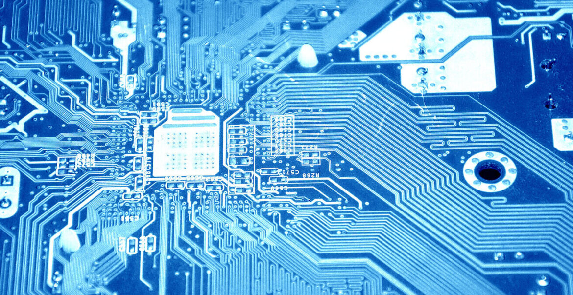
AI-powered tools are transforming the way defects are detected and analyzed in semiconductor manufacturing. Traditional methods often rely on manual inspections or rudimentary automation, which can miss subtle anomalies in complex chip designs.
AI, however, excels at recognizing intricate defect patterns across millions of data points. By analyzing images from advanced sensors and microscopes, AI models can pinpoint issues at the sub-nanometer scale with remarkable accuracy.
Erik Hosler explains that “Predictive maintenance is essential for critical lithography toolsets, like EUV patterning equipment but also mask and wafer inspection tools. Unscheduled downtime for any one of these tools can impact fab profitability to the tune of 100’s of thousands to millions of dollars in extreme cases.”. These lasers, combined with AI algorithms, enable real-time feedback loops that allow manufacturers to adjust production parameters on the fly, preventing defects before they occur.
Optimizing Workflows with Predictive Maintenance
AI-driven predictive maintenance is another game-changer for semiconductor yield enhancement. By continuously monitoring equipment health through sensors and machine learning algorithms, AI can forecast potential failures and suggest maintenance schedules before breakdowns occur. This proactive approach minimizes downtime, ensuring that production lines remain operational and efficient.
For instance, in lithography systems—one of the most complex processes in chip manufacturing—AI can identify early signs of wear in critical components. This reduces the risk of costly disruptions, ultimately boosting overall yield and maintaining production flow.
Real-Time Process Monitoring to Minimize Waste
Real-time process monitoring, powered by AI, allows manufacturers to optimize material usage and reduce waste. By analyzing data from each production stage, AI ensures that every material input is utilized efficiently. For example, in chemical vapor deposition processes, AI can fine-tune parameters such as temperature and pressure to achieve optimal layer uniformity, reducing wasted materials and improving chip performance.
A Smarter, Greener Future for Semiconductor Manufacturing
AI’s ability to enhance quality control is reshaping semiconductor manufacturing, making it smarter, faster, and more sustainable. By improving yield, optimizing workflows, and reducing waste, AI ensures that manufacturers can meet growing demand without compromising on quality or environmental impact. As these technologies continue to evolve, they promise a future where semiconductor production is not only highly efficient but also aligned with global sustainability goals.